- 您现在的位置:买卖IC网 > Sheet目录368 > W631GG6KB-15 (Winbond Electronics)IC DDR3 SDRAM 1GBIT 96WBGA
�� �
�
�W631GG6KB�
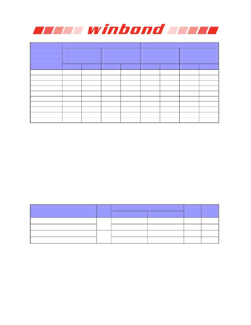
�Table� 20� –� Allowed� time� before� ringback� (t� DVAC� )� for� CK� -� CK#� and� DQS� -� DQS#�
�DDR3-1333/1600�
�DDR3-1866�
�Slew� Rate�
�[V/nS]�
�t� DVAC� [pS]�
�@� V� IH/LDIFF(AC)� =�
�350mV�
�t� DVAC� [pS]�
�@� V� IH/LDIFF(AC)� =�
�300mV�
�t� DVAC� [pS]�
�@� V� IH/LDIFF(AC)� =�
�300mV�
�t� DVAC� [pS]�
�@� V� IH/LDIFF(AC)� =�
�(CK� -� CK#)� only�
�Min.�
�Max.�
�Min.�
�Max.�
�Min.�
�Max.�
�Min.�
�Max.�
�>� 4.0�
�4.0�
�3.0�
�2.0�
�1.8�
�1.6�
�1.4�
�1.2�
�1.0�
�<� 1.0�
�75�
�57�
�50�
�38�
�34�
�29�
�Note�
�Note�
�Note�
�Note�
�-�
�-�
�-�
�-�
�-�
�-�
�-�
�-�
�-�
�-�
�175�
�170�
�167�
�119�
�102�
�81�
�54�
�19�
�Note�
�Note�
�-�
�-�
�-�
�-�
�-�
�-�
�-�
�-�
�-�
�134�
�134�
�112�
�67�
�52�
�33�
�9�
�Note�
�Note�
�Note�
�-�
�-�
�-�
�-�
�-�
�-�
�-�
�-�
�-�
�-�
�139�
�139�
�118�
�77�
�63�
�45�
�23�
�Note�
�Note�
�Note�
�-�
�-�
�-�
�-�
�-�
�-�
�-�
�-�
�-�
�-�
�Note:�
�Rising� input� differential� signal� shall� become� equal� to� or� greater� than� V� IHDIFF(AC)� level� and� Falling� input� differential� signal� shall�
�become� equal� to� or� less� than� V� ILDIFF(AC)� level.�
�10.6.4� Single-ended� requirements� for� differential� signals�
�Each� individual� component� of� a� differential� signal� (CK,� DQSL,� DQSU,� CK#,� DQSL#,� DQSU#)� has� also�
�to� comply� with� certain� requirements� for� single-ended� signals.�
�CK� and� CK#� have� to� approximately� reach� V� SEH� min� /� V� SEL� max� (approximately� equal� to� the� AC-levels�
�(V� IH.CA(AC)� /� V� IL.CA(AC)� )� for� ADD/CMD� signals)� in� every� half-cycle.�
�DQSL,� DQSU,� DQSL#,� DQSU#� have� to� reach� V� SEH� min� /� V� SEL� max� (approximately� the� AC-levels�
�(V� IH.DQ(AC)� /� V� IL.DQ(AC)� )� for� DQ� signals)� in� every� half-cycle� preceding� and� following� a� valid� transition.�
�Note� that� the� applicable� ac-� levels� for� ADD/CMD� and� DQ‘s� might� be� differ� ent� per� speed-bin� etc.� E.g.,� if�
�V� IH.CA(AC150)� /V� IL.CA(AC150)� is� used� for� ADD/CMD� signals,� then� these� AC-levels� apply� also� for� the�
�single-ended� signals� CK� and� CK#.�
�Table� 21� –� Single-ended� levels� for CK, DQSL, DQSU, CK#, DQSL# o� r� DQSU#�
�PARAMETER�
�SYM.�
�DDR3-1333,� DDR3-1600� &� DDR3-1866�
�MIN.� MAX.�
�UNIT�
�NOTES�
�Single-ended� high� level� for� strobes�
�Single-ended� high� level� for� CK,� CK#�
�Single-ended� low� level� for� strobes�
�Single-ended� low� level� for� CK,� CK#�
�V� SEH�
�V� SEL�
�(V� DD� /2)� +� 0.175�
�(V� DD� /2)� +� 0.175�
�Note� 3�
�Note� 3�
�Note� 3�
�Note� 3�
�(V� DD� /2)� -� 0.175�
�(V� DD� /2)� -� 0.175�
�V�
�V�
�V�
�V�
�1,� 2�
�1,� 2�
�1,� 2�
�1,� 2�
�Notes:�
�1.� For� CK,� CK#� use� V� IH.CA(AC)� /� V� IL..CA(AC)� of� ADD/CMD;� for� strobes� (DQSL,� DQSL#,� DQSU,� DQSU#)� use� V� IH.DQ(AC)� /�
�V� IL.DQ(AC)� of� DQs.�
�2.� V� IH.DQ(AC)� /� V� IL.DQ(AC)� for� DQs� is� based� on� V� REFDQ� ;� V� IH.CA(AC)� /� V� IL.CA(AC)� for� ADD/CMD� is� based� on� V� REFCA� ;� if� a�
�reduced� AC-high� or� AC-low� level� is� used� for� a� signal� group,� then� the� reduced� level� applies� also� here.�
�3.� These� values� are� not� defined;� however,� the� single-ended� signals� CK,� CK#,� DQSL,� DQSL#,� DQSU,� DQSU#� need� to� be� within�
�the� respective� limits� (V� IH(DC)� max,� V� IL(DC)min� )� for� single-ended� signals� as� well� as� the� limitations� for� overshoot� and�
�undershoot.� Refer� to� section� 10.12� “� Overshoot� and� Undershoot� Specifications� ”� on� page� 121.�
�Publication� Release� Date:� Dec.� 09,� 2013�
�Revision� A05�
�-� 104� -�
�发布紧急采购,3分钟左右您将得到回复。
相关PDF资料
W9412G6IH-5
IC DDR-400 SDRAM 128MB 66TSSOPII
W9412G6JH-5I
IC DDR SDRAM 128MBIT 66TSOPII
W9425G6EH-5
IC DDR-400 SDRAM 256MB 66TSSOPII
W9425G6JH-5I
IC DDR SDRAM 256MBIT 66TSOPII
W947D2HBJX5E
IC LPDDR SDRAM 128MBIT 90VFBGA
W948D2FBJX5E
IC LPDDR SDRAM 256MBIT 90VFBGA
W949D2CBJX5E
IC LPDDR SDRAM 512MBIT 90VFBGA
W971GG6JB25I
IC DDR2 SDRAM 1GBIT 84WBGA
相关代理商/技术参数
W631GG8KB-11
制造商:Winbond Electronics Corp 功能描述:IC DDR3 SDRAM 1GBIT 制造商:Winbond Electronics Corp 功能描述:IC DDR3 SDRAM 1GBIT 78WBGA
W631GG8KB-12
制造商:Winbond Electronics Corp 功能描述:DRAM Chip DDR3 SDRAM 1G-Bit 128Mx8 1.5V 制造商:Winbond Electronics Corp 功能描述:IC DDR3 SDRAM 1GBIT 制造商:Winbond Electronics Corp 功能描述:IC DDR3 SDRAM 1GBIT 78WBGA
W631GG8KB-15
制造商:Winbond Electronics Corp 功能描述:IC DDR3 SDRAM 1GBIT 制造商:Winbond Electronics Corp 功能描述:IC DDR3 SDRAM 1GBIT 78WBGA
W632
制造商:LUMINIS 制造商全称:LUMINIS 功能描述:Wall mount
W632GG6KB-11
制造商:Winbond Electronics Corp 功能描述:IC DDR3 SDRAM 2GBIT 96WBGA
W632GG8KB-11
制造商:Winbond Electronics Corp 功能描述:IC DDR3 SDRAM 2GBIT 78WBGA
W634
制造商:LUMINIS 制造商全称:LUMINIS 功能描述:Wall mount
W638
制造商:LUMINIS 制造商全称:LUMINIS 功能描述:Wall mount